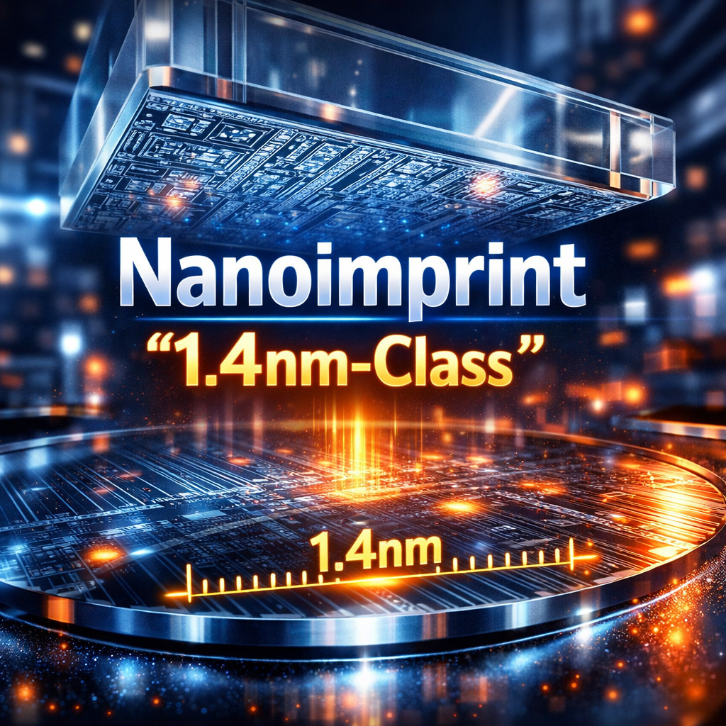
Recently, Dai Nippon Printing Co., Ltd. (DNP) announced that it has successfully developed a nanoimprint lithography (NIL) template with circuit line widths as fine as 10nm. The company says this template can be used to pattern logic semiconductor circuitry at a level comparable to the 1.4nm node—supporting continued miniaturization for advanced logic used in smartphones, data centers, and NAND flash-related applications.
DNP plans to showcase the new template at SEMICON Japan 2025, taking place from December 17 to 19, 2025 at Tokyo Big Sight.
Nanoimprint Advances Point to “1.4nm-Class” Patterning
As global demand for computing power continues to climb, the push for ever-smaller, more capable semiconductors has accelerated. This trend has helped drive ongoing progress in extreme ultraviolet (EUV) lithography-based chip production.
At the same time, EUV remains expensive and energy-intensive. With EUV tools carrying extremely high price tags and requiring significant power during exposure, the industry has been looking for practical alternatives that can lower manufacturing costs while reducing environmental impact.
Against this backdrop, Canon—after losing ground to ASML in the lithography equipment market—has spent more than a decade working with key Japanese ecosystem partners, including DNP, to develop nanoimprint-based approaches.
What NIL Is, and Why It Matters
Nanoimprint lithography differs from conventional optical projection lithography. Instead of projecting and reducing an image through optics, NIL works more like advanced printing: it physically presses a patterned template to form features directly on the wafer.
In principle, a single imprint can create complex 2D or 3D patterns at precise locations. This can simplify certain patterning steps and potentially reduce reliance on EUV for some advanced processes, helping to cut both equipment procurement and manufacturing costs.
In October 2023, Canon officially introduced its NIL-based semiconductor manufacturing tool, the FPA-1200NZ2C, positioning it as a lower-cost pathway for advanced-node production.
Cost and Energy: NIL’s Core Value Proposition
According to Canon’s positioning, NIL equipment targets sub-10nm manufacturing and can reach down to 5nm-class production in certain applications. Compared with today’s commercialized EUV lithography, NIL is generally slower in throughput, but it is promoted as significantly more energy-efficient and far less expensive to purchase.
Canon has previously stated that its nanoimprint systems could reduce chip manufacturing energy consumption by roughly 90%, and cut equipment procurement costs by about 90% versus EUV—framing NIL as a compelling option for cost-sensitive advanced manufacturing.
However, EUV is a mature, widely adopted solution with strong ecosystem support, so NIL has faced clear competitiveness challenges. Looking forward, as the industry enters the angstrom era and High-NA EUV drives manufacturing costs even higher, NIL’s potential would become more prominent if it can scale to comparable patterning requirements.
The Template Challenge: The Key to NIL Scaling
For nanoimprint lithography, the achievable process level is tightly linked to the quality and resolution of the imprint template.
Unlike optical lithography—which can reduce and scale projected patterns—NIL requires 1:1 pattern transfer across a template chain (for example, master template to replica templates to working templates). Each step can introduce defects, making yield, defect control, and repeatability critical.
When feature sizes move below 20nm, template fabrication typically depends on state-of-the-art multi-beam mask writing (MBMW) systems. As dimensions shrink further, complexity rises sharply—putting more pressure on cost, yield, and manufacturability.
DNP’s 10nm NIL Template: How It Was Made
DNP has been developing NIL templates since 2003, building process expertise aimed at reducing exposure energy by transferring circuit patterns directly onto substrates via imprinting.
Now, DNP says it has achieved a 10nm line-width NIL template—positioned as comparable to the 1.4nm node—potentially enabling substitution for parts of EUV, and even High-NA EUV, in certain advanced logic manufacturing flows where cost control is a priority.
DNP notes that by providing this template, it can broaden customers’ process options, helping reduce manufacturing costs and lessen environmental impact.
To realize the 10nm line-width miniaturization, DNP used self-aligned double patterning (SADP). This technique increases pattern density by depositing thin films and performing etch steps on top of a pattern formed by lithography, effectively doubling the density of the features.
Roadmap: Evaluation Now, Mass Production Targeted for 2027
DNP says it is currently engaging with semiconductor manufacturers and other customers, and has already begun evaluation work for the NIL templates. The company is targeting the start of mass production in 2027.
Looking ahead, DNP plans to continue advancing NIL template development and strengthen its production capabilities to meet growing demand. It also aims to increase NIL-related sales to 4 billion yen by fiscal 2030 as part of its longer-term business growth plan.