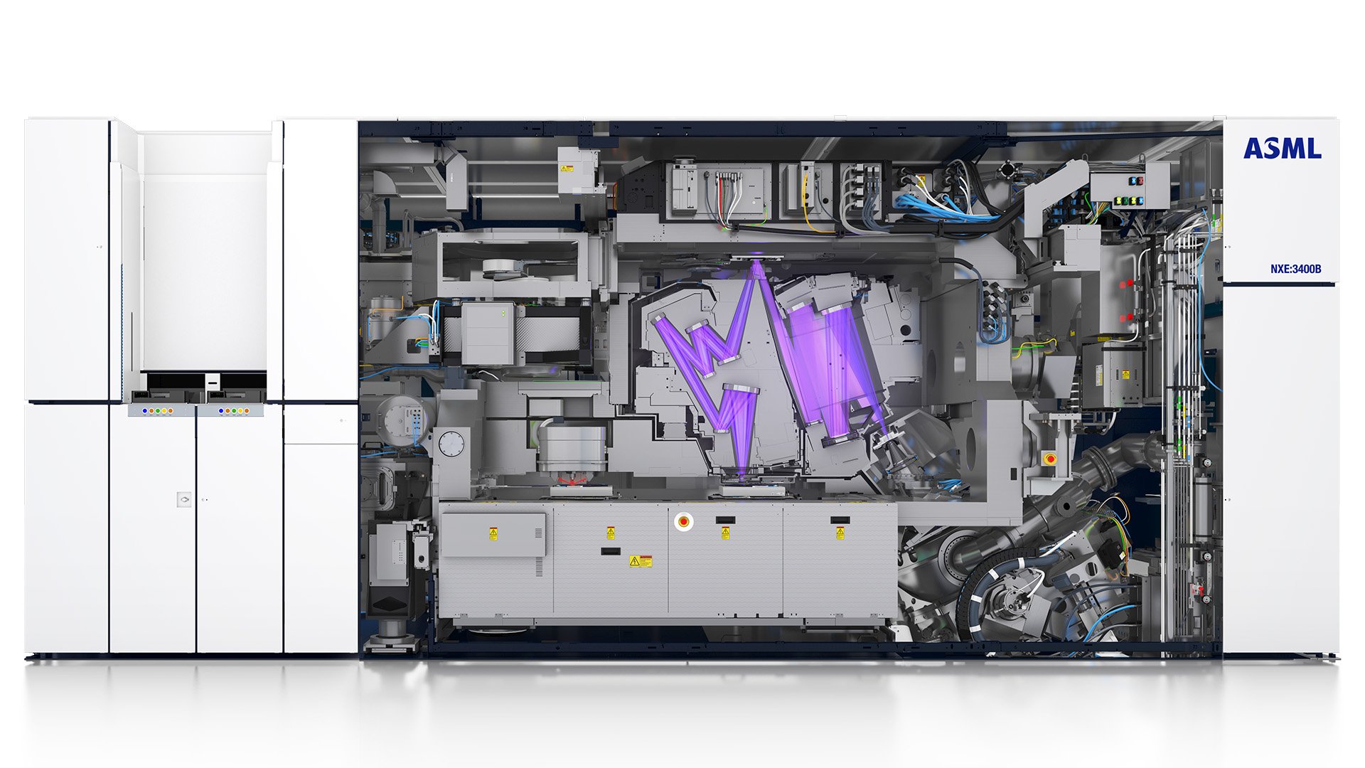
Substrate’s Bold Move: U.S. Startup Claims Breakthrough X-Ray Lithography to Rival ASML’s EUV and Challenge TSMC’s AI Chip Dominance
American semiconductor startup Substrate has shaken up the global chip industry with a bold announcement: the company claims its new X-ray exposure technology can achieve 12-nanometer patterning on 300mm wafers — and is already eyeing the 2-nanometer node. The breakthrough reportedly eliminates the need for multiple exposures, potentially reducing chip manufacturing costs by an entire order of magnitude, while offering a resolution that directly rivals ASML’s world-leading EUV lithography machines.
Substrate also revealed plans to build its own wafer fabrication plant in the U.S. by 2028, with an initial investment in the “several billion dollars” range. The move signals its intent to challenge TSMC’s dominance in AI chip manufacturing, taking aim at both ASML and TSMC in one sweeping strategy.
From a technical perspective, the startup says its X-ray lithography has already proven capable of achieving 12nm feature sizes on silicon wafers and could scale further to 2nm nodes. Unlike traditional photolithography, this approach bypasses complex multiple-exposure steps, promising faster throughput and dramatically lower production costs.
However, despite its ambitious claims, Substrate’s technology has not yet been independently verified. Industry observers caution that the real-world performance, yield rates, and long-term stability of the equipment remain to be proven.
On the financial side, Substrate has already raised $100 million in seed funding, earning a valuation exceeding $1 billion — officially joining the ranks of semiconductor unicorns. Backing the company are some of the most influential names in venture capital, including Peter Thiel’s Founders Fund, General Catalyst, and In-Q-Tel, the venture arm supported by the CIA.
Its team composition is equally impressive, drawing experts from TSMC, IBM, Google, and various U.S. national laboratories. This cross-disciplinary talent base covers chip design, manufacturing, and advanced materials — giving Substrate a credible foundation for both R&D and future fab operations.
According to Substrate’s roadmap, the first fab network will break ground in 2028, with construction costs far below today’s advanced fab investments that often exceed $20 billion per site. The company’s goal is to enter high-end semiconductor production with a leaner, more cost-efficient approach.
Currently, ASML’s EUV lithography systems hold a near-total monopoly in advanced chip manufacturing, serving giants like TSMC and Samsung. If Substrate’s X-ray lithography proves viable, it could redefine the global semiconductor landscape, shaking the very foundations of the existing supply chain.
Still, skepticism persists. Bernstein analyst David Dai noted that X-ray lithography is not an entirely new concept — major companies, including ASML itself, explored it in the past without success. For Substrate to succeed, it must overcome major hurdles related to yield consistency, system stability, and ecosystem compatibility.
Moreover, the company’s tools have not yet undergone real-world validation in mainstream fabs, and its customer network and supplier partnerships remain in early development. These practical challenges could slow or even derail its ambitious plans to disrupt the industry.
As global demand for advanced chips surges — driven by artificial intelligence and high-performance computing — Substrate’s claims introduce an exciting new variable into the semiconductor race. Whether this emerging contender can truly “break ASML’s monopoly” will depend on one thing: turning bold promises into proven technology.